Materials

Twelve substrates,
0.12 µm to 25 µm.

Every material below is sourced through a qualified global network, prepared for yield, and carried with full batch and lot traceability. Pick by wavelength first, then by environment and cost.

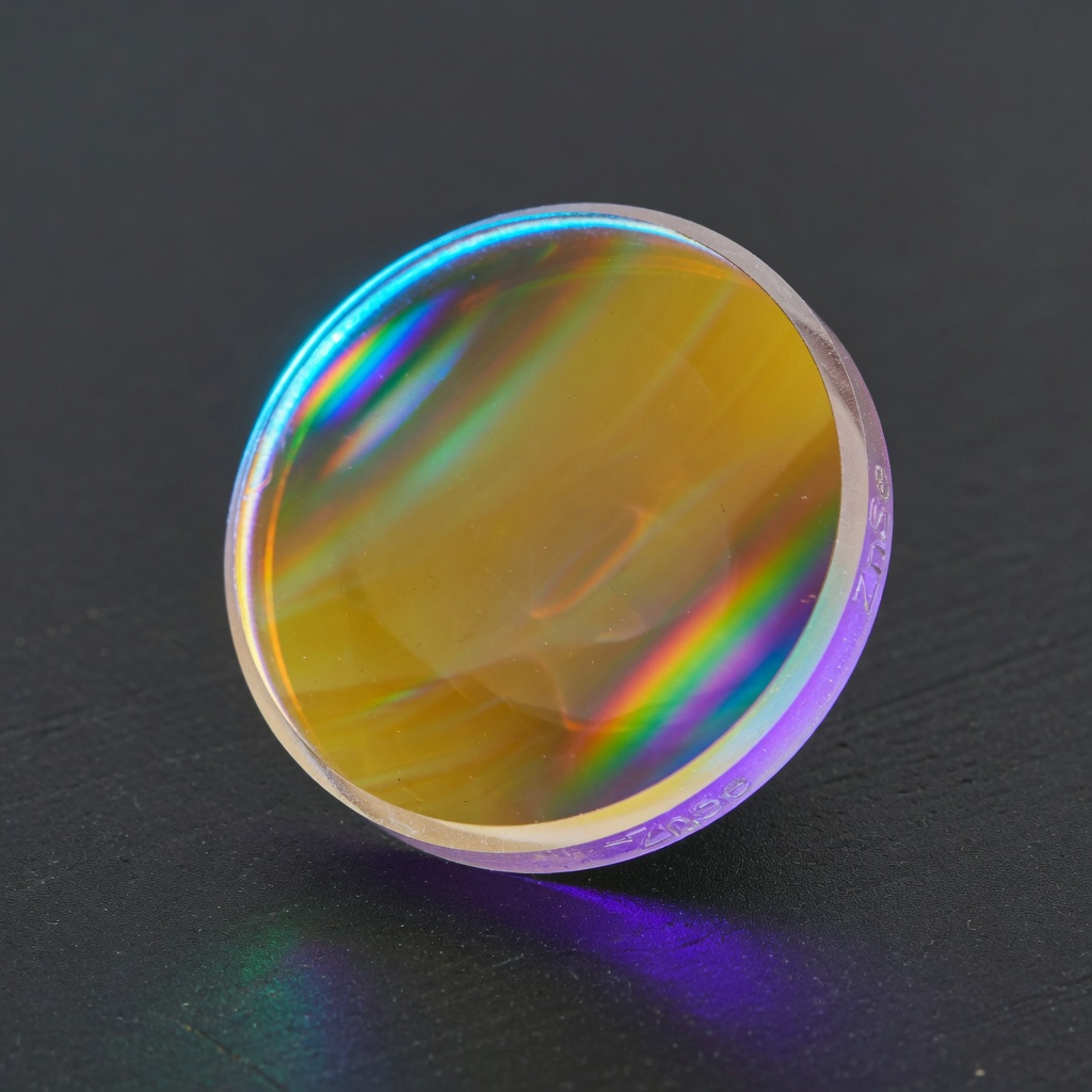
Illustrative ZnSe precision optic close-up with coating iridescence.
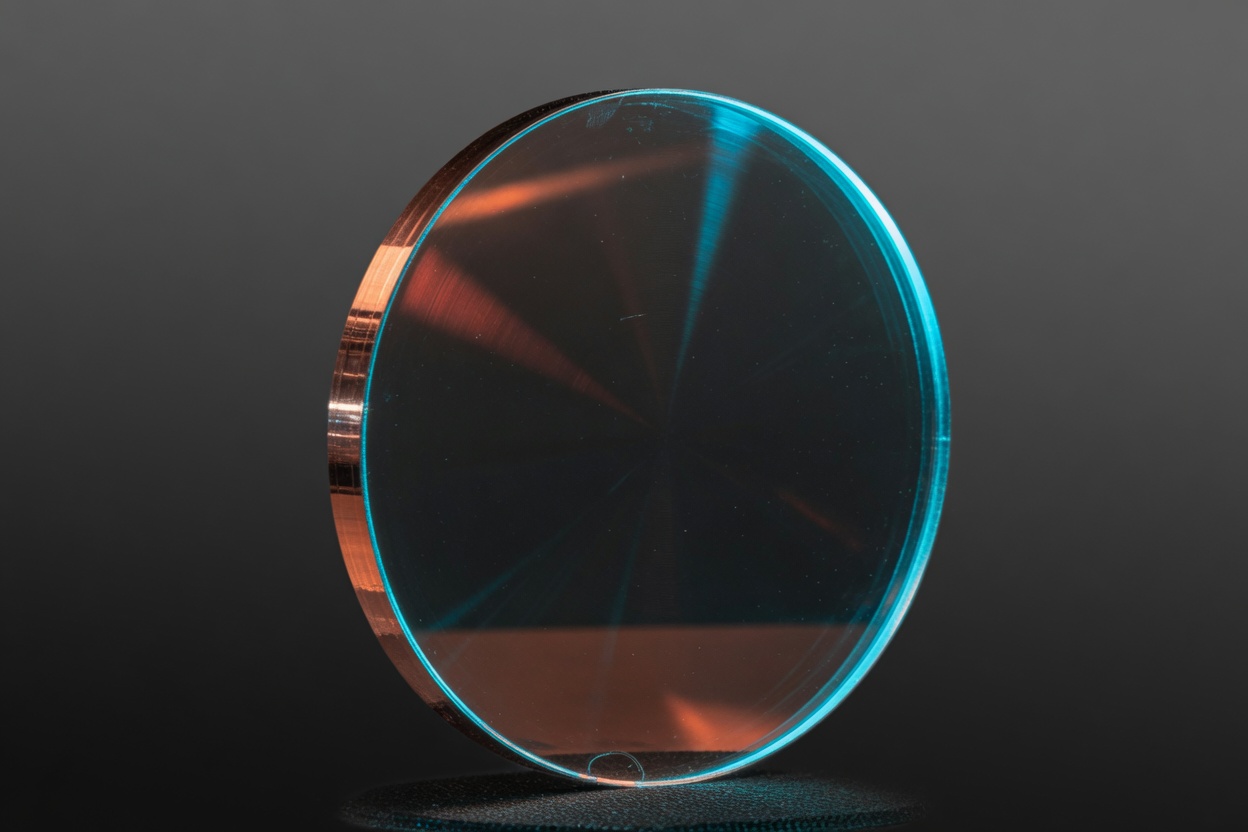
Illustrative copper mirror substrate for high-power beam delivery.
Comparison

Material matrix.

Typical published values for common grades. Confirm against a grade-specific datasheet before design freeze.

Comparison of optical materials by transmission range, refractive index, density and Knoop hardness
Material Transmission Refractive index Density Knoop hardness Typical use
MgF₂0.12 – 7 µm1.3777 @ 0.6 µm3.18 g/cm³415Deep-UV and excimer windows
CaF₂0.13 – 10 µm1.4338 @ 0.6 µm3.18 g/cm³158Broadband UV–IR, FTIR cells
Sapphire0.17 – 5.5 µm1.7682 @ 0.6 µm3.98 g/cm³2200Abrasion and pressure windows
Fused Silica0.18 – 2.5 µm1.4585 @ 0.59 µm2.20 g/cm³500UV/VIS/NIR laser optics
N-BK70.35 – 2 µm1.5168 @ 0.59 µm2.51 g/cm³610General visible optics
ZnS (multispectral)0.4 – 14 µm2.2008 @ 10.6 µm4.09 g/cm³160Dual-band VIS + LWIR
ZnSe0.6 – 21 µm2.4028 @ 10.6 µm5.27 g/cm³120CO₂ laser optics
Chalcogenide (AMTIR-1)0.7 – 12 µm2.5109 @ 10.6 µm4.40 g/cm³170Athermal thermal imaging
GaAs1 – 15 µm3.278 @ 10.6 µm5.32 g/cm³731High-power CO₂ delivery
Silicon1.2 – 8 µm3.4223 @ 5 µm2.33 g/cm³1150MWIR windows, mirror blanks
Germanium2 – 14 µm4.0032 @ 10.6 µm5.33 g/cm³780Thermal imaging objectives
Copper (mirror)R > 98% @ 10.6 µm8.96 g/cm³High-power beam steering

Knoop hardness is a relative guide to handling and cleaning risk — ZnSe and CaF₂ are soft and scratch easily; sapphire and silicon tolerate far more.


Infrared semiconductors

The long-wave workhorses.

ZnSe · Zinc Selenide

Zinc Selenide

CVD-grown, laser grade with ≤ 80 µm inclusions. Very low absorption at 10.6 µm makes it the default focusing and window material for CO₂ systems, and its visible transmission gives you a red alignment channel through the same optic.

  • Transmission0.6 – 21 µm
  • n @ 10.6 µm2.4028
  • Density5.27 g/cm³
  • Knoop120 — soft

Handle with care: the low hardness means fingerprints and aggressive cleaning leave permanent marks. Specify AR both surfaces for a real transmission gain.

Ge · Germanium

Germanium

The highest refractive index of the common IR set, which buys you shorter, more compact lens designs. Opaque in the visible, so alignment must be handled on a separate path.

  • Transmission2 – 14 µm
  • n @ 10.6 µm4.0032
  • Density5.33 g/cm³
  • Knoop780
Thermal runaway: transmission degrades sharply above roughly 100 °C. Tell us the operating temperature at quote so we can flag it before you design it in.
Si · Silicon

Silicon

Less than half the density of germanium and a much better thermal conductor — the right call whenever mass or heat dissipation drives the design. Also our standard blank for laser mirror substrates.

  • Transmission1.2 – 8 µm
  • n @ 5 µm3.4223
  • Density2.33 g/cm³
  • Knoop1150 — hard

Note the strong lattice absorption band near 9 µm — silicon is a MWIR material, not an LWIR one.

GaAs · Gallium Arsenide

Gallium Arsenide

Mechanically robust with a high damage threshold — chosen for high-power CO₂ delivery optics and protective windows that live in dirty, high-flux environments where ZnSe would not survive handling.

  • Transmission1 – 15 µm
  • n @ 10.6 µm3.278
  • Density5.32 g/cm³
  • Knoop731
ZnS · Zinc Sulfide

Zinc Sulfide

Available as Cleartran® and multispectral grades. The unusually wide window — visible right through long-wave IR — makes it the natural substrate for dual-band assemblies that must image and align through one element.

  • Transmission0.4 – 14 µm
  • n @ 10.6 µm2.2008
  • Density4.09 g/cm³
  • Knoop160
AMTIR-1 · Chalcogenide

Chalcogenide Glass

A germanium–arsenic–selenium glass with a very low thermo-optic coefficient. If a thermal imager has to hold focus across its whole operating temperature range without an active compensation mechanism, this is how it is done.

  • Transmission0.7 – 12 µm
  • n @ 10.6 µm2.5109
  • Density4.40 g/cm³
  • AdvantageAthermal · mouldable

Ultraviolet & visible

The short-wave end.

Alignment paths, beam combiners, visible channels in dual-band assemblies, and everything that has to survive an excimer source.

Fused Silica · SiO₂

Low thermal expansion and excellent UV transmission. The default for Nd:YAG harmonics and any high-stability visible path.

  • Range0.18 – 2.5 µm
  • n @ 0.59 µm1.4585

Calcium Fluoride · CaF₂

The widest single window we stock — deep UV all the way to 10 µm. Standard for FTIR cells and broadband spectroscopy.

  • Range0.13 – 10 µm
  • n @ 0.6 µm1.4338

Magnesium Fluoride · MgF₂

Transmits further into the vacuum UV than anything else here, and is birefringent — specify orientation if that matters.

  • Range0.12 – 7 µm
  • n @ 0.6 µm1.3777

Sapphire · Al₂O₃

Knoop 2200 — effectively unscratchable in service. The answer for abrasive, high-pressure or chemically hostile windows.

  • Range0.17 – 5.5 µm
  • n @ 0.6 µm1.7682

Reflective optics

Copper mirrors.

Past a certain power density no transmissive optic survives the thermal load. Diamond-turned copper reflects more than 98% at 10.6 µm and carries the remaining heat away through the substrate — with a water-cooled option for continuous-duty industrial sources.

  • Reflectance> 98% @ 10.6 µm
  • Density8.96 g/cm³
  • FinishDiamond-turned
  • OptionsWater-cooled · protected coat
Not sure which material?

Tell us the wavelength.

Send the source wavelength, power, environment and quantity. We will recommend a substrate and coating design before you commit to a drawing.